Client Overview
A confidential Fortune 500 semiconductor manufacturer faced significant challenges in particle tracking and defect analysis across its complex multi-step fabrication process. With 10-12 sequential process steps, the company needed to improve quality control while maintaining production efficiency in a highly technical manufacturing environment.
Key takeaways
03- 01Defect analysis time dropped by over 90% — minutes instead of hours.
- 02Visual language models classify defects automatically across every fabrication stage.
- 03Particle-migration mapping traces a defect's origin across all 10–12 process steps.
Challenges
The manufacturer encountered several critical operational hurdles:
- Manual Inspection Bottlenecks: Engineers spent hours manually inspecting part images, classifying defects, and tracing particle origins across multiple fabrication stages, creating analysis delays.
- Scalability Limitations: The error-prone manual process couldn't scale across production lines, restricting responsiveness to quality issues.
- Traceability Gaps: Difficulty tracking defect migration through sequential processes hindered root cause identification and impacted yield rates.
Use Cases
The semiconductor company prioritized key applications for AI-driven defect analysis:
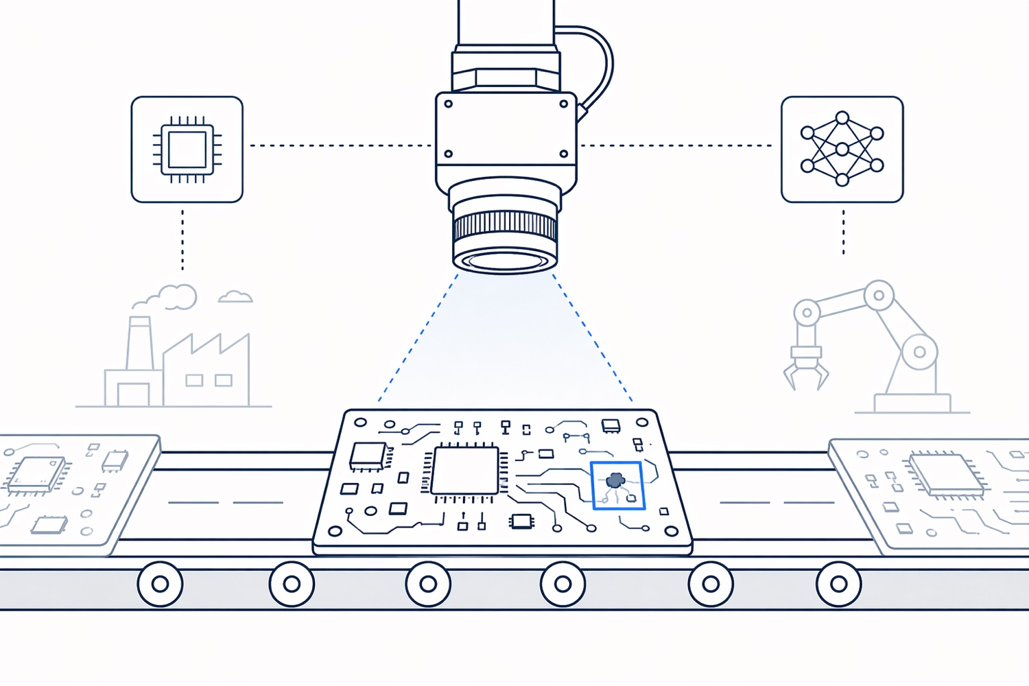
- Automated Defect Classification: Rapid identification and categorization of defects across different process stages
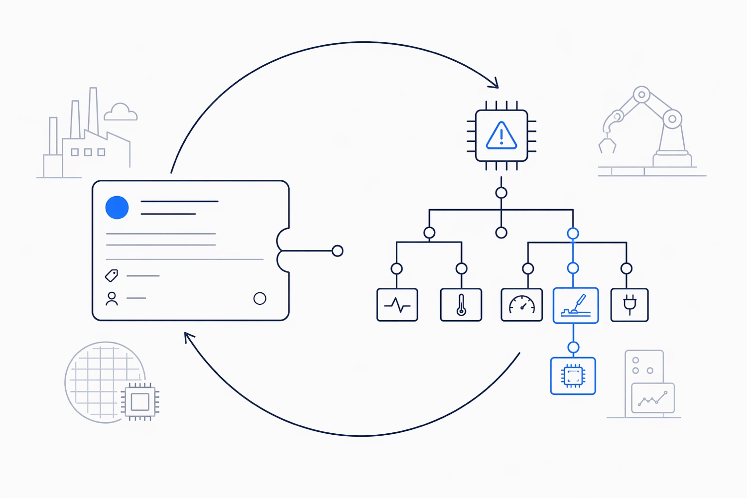
- Particle Migration Tracking: Tracing defect origins and progression through sequential fabrication steps
- Root Cause Analysis: Generating high-confidence suggestions for defect sources to accelerate remediation
Solution: TIA Studio Platform
ThirdAI's AI-powered defect analysis solution delivered transformative capabilities:
- Visual Language Models: Leveraged advanced computer vision to automatically analyze and classify defects in manufacturing images
- Automated Defect Triage: Implemented end-to-end workflow automation from detection to root cause suggestion
- Process Traceability Mapping: Created visual migration paths showing particle movement across production stages
Defect analysis that once took hours now completes in minutes — over 90% faster.
Key Outcomes
- Dramatic Time Reduction: Achieved over 90% time savings with defect analysis completing in minutes instead of hours
- Enhanced Traceability: Established clear defect migration paths across process steps enabling proactive interventions
- Resource Optimization: Freed engineers from manual inspection to focus on strategic process improvements and yield optimization
Beyond raw speed, mapping particle migration across every process step turns defect analysis from reactive inspection into proactive, yield-focused intervention — engineers act before a defect propagates down the line.
Conclusion
The implementation of ThirdAI's TIA Studio platform transformed defect analysis from a manual, time-intensive process to an automated, insight-driven workflow. By providing rapid root cause identification and complete defect journey mapping, the semiconductor manufacturer established new standards for quality control efficiency while creating a foundation for continuous process optimization.
Contact us to book your free demo today!
Meet our engineers to explore how ThirdAI Automation can support your manufacturing excellence programs.